
China Could be Close to Replicate ASML’s Latest EUV Chip Making Machine
In an exclusive article by Reuters published on 18 December 2025, which was then taken up by media outlets around the world, it is reported that China might be closer to closing the gap in advanced semiconductor manufacturing than was previously thought. Indeed, anonymous sources revealed that China has completed a prototype of the Extreme Ultraviolet (#EUV) photolithography machine in a secret lab in Shenzhen, also known as the Silicon Valley of China. Some analysts likened the effort to the Manhattan Project, which gave the US the nuclear bomb.
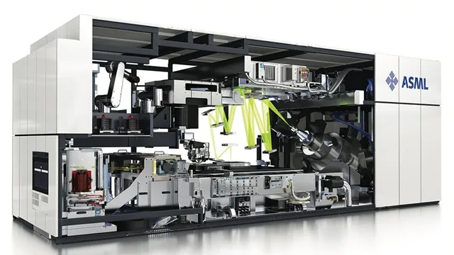
The prototype was reverse-engineered thanks to former ASML engineers, mostly Chinese nationals, and occupies a whole floor. Currently, the state-of-the-art by ASML is actually the size of a bus. The prototype cannot produce #chips yet but China has set a target of 2028 to match the capabilities of ASML.
The level of secrecy is such that the exact location of the lab is unknown and employees refer to each other using aliases instead of real names. Certain observers note that the facility is probably linked with SMIC or Huawei, which has long tried and invested heavily to close the technology gap.
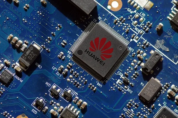
SMIC is reported to have mastered the 5-nm technology chip production. Since 2024, it was rumored that Huawei has been putting great efforts in developing 3-nm chips using a hack on older-generation Deep Ultraviolet (DUV) equipment. What is known is that Huawei does have the capability to produce 5-nm chips at scale.
When hit by an embargo on the smartphone operating system Android OS, Huawei came up its own Harmony OS. Similarly, faced with restrictions on certain key chips for smartphones, Huawei has managed to find alternative sources.
One of the key components of photolithography is the necessity of precision optics, which #ASML sources from German company Carl-Zeiss. It is worth noting that Huawei has also partnered with Karl-Zeiss for the camera lens on its top-of-the-line smartphones.
In 2025, the 2-nm is the bleeding edge, although 3-nm is the leading technology for high-volume production. So far, only Taiwan Semiconductor Manufacturing Company (#TSMC), South Korea’s Samsung, and America’s Intel have production capabilities for 2-nm. It is reported that Nvidia’s top #AI chip, the Blackwell B200 and one-generation older Hopper H200 GPU are based on the 4-nm technology.
Previously, some experts believed that China was at least a couple of generations behind #ASML, and that it would take decades to catch up. The existence of the prototype might cause a revision of the evaluation to size up the gap in years instead of decades.
For decades, the West has restricted the export of its latest technology products to prevent China from getting its hand on the latest EUV photolithography machine. Amidst the trade war between US and China, the US even imposed chip maker Nexperia, causing a temporary shortage.
On the other hand, China holds a dominant position in the supply chain for germanium and gallium, which are #CriticalMinerals that go into semiconductors. Therefore, the US and China are in a cat-and-mouse game for semiconductor supremacy. Both are scrambling to build up a whole semiconductor ecosystem within their borders.
Just recently on 13 December 2025, the US announced the establishment of a semiconductor alliance, dubbed #PaxSilica, to ensure its leadership in this key technology sector. Certain analysts believed that the information was intentionally leaked by the Chinese Government in response to Pax Silica.